|
|
|
THEORETICAL INFORMATION | ||||||||||||||||||||||||||||||||||||||||||||||||||||||||||||||||||||||
|
The
insertion method can be used to characterise a filter response in microwave.
It is defined as the ratio of power available from source to power delivered
to load. In this program two common types of filter characteristics are
used: maximally flat and equal ripple (or Chebyshev) filters. MAXIMALLY
FLAT FILTER:
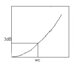
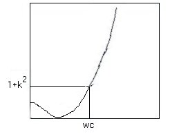
Figure 1:Low-pass filter response for maximally flat filter.Frequency vs power loss EQUAL RIPPLE (CHEBYSHEV):It provides a sharper cut off , however the pass band has ripples of amplitude 1+k2. It is specified by
Figure 2: Low-pass filter response for equal ripple filter. Frequency vs power loss LOW-PASS FILTER DESIGN Ladder circuits, as shown below, gives the power loss characteristics of those filter types. The lumped circuit elements are shunt capacitors and series inductors as shown in figure 3. For maximally flat or equal ripple response in the pass band, the ladder network is symmetric for odd number of elements. If we let Zin be the input impedance seen from Rs, then reflection coefficient is
Then, power loss ratio becomes
At
w=0, all capacitors open and all inductors short circuit , and hence Zin=1.
PLR is zero for maximally flat and equal ripple filter when
N is odd. For equal ripple with N is even PLR=1+k2
at w=0.
For maximally flat filter with a power loss ratio
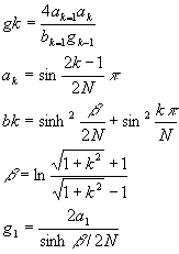
Some numerical
values of gk for maximally flat filter listed up to N =5 in table 1.
Equal ripple low pass filter element values can be calculated by gN+1=1 N odd when element gN is a capacitor gN+1=R, but when gN is an inductor gN+1=1/R.
Some numerical values of gk for equal ripple filter N up to 5 are listed in table 2.
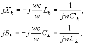
FILTER TRANSFORMATION:The low pass prototype element values which are calculated for R=1 and wc=1 can be modified for arbitrary source impedance and cut off frequency. In addition, by frequency transformation, band pass and high pass filter element values can be obtained or vice versa.Impedance and Frequency Transformation: Element values calculated for wc=1 and R=1 can be transformed for arbitrary cut off frequency wc and source impedance R0 by using following simple equations L� =R0L/wc (10)
which shows that the series inductors must be replaced with capacitors C�k and the shunt capacitors must be replaced with inductors L�k given by
Then new
ladder network is shown in figure 4.
figure 4: high pass filter ladder network Low pass to Band pass Transformation:w=0 is mapped
to w=wo, meaning that pass band of low pass filter is now centred around
wo. Cut off frequency 1 mapped to the edge frequencies w=w1 and w=w2 as
desired for a band pass filter. Similarly, new element values are determined
by
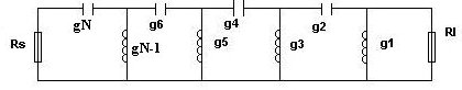
Above equations show that the series inductor Lk is transformed to a series LC circuit with element values,
and the shunt capacitor Ck is transformed to a shunt LC circuit with element values,
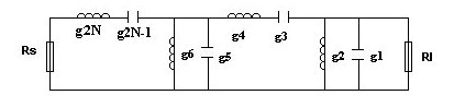
figure 5: band pass filter circuit.
Approximate
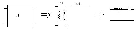
Equivalent Circuits for short section transmission line:
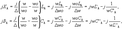
the series elements of T equivalent circuit are given by
and shunt element value is Z12. The equivalent circuit (see figure 6) has the following element values: B=sin(b l )/Zo B~0, B~Yob
l, 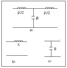
a) T equivalent circuit for a TLb) Equivalent circuit for smallbl and large Zo c) Equivalent circuit for small b l and small Zo A typical
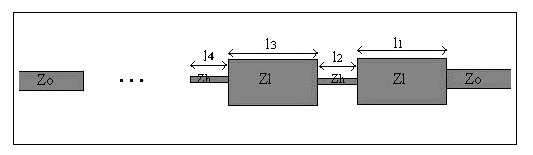
to view of the stepped impedance low pass filter can be seen in figure
2. For high pass filter it is just replacing high impedance lines with
low impedance transmission line section and element values transformed.
figure 7: Microstrip layout of low pass filter COUPLED LINE FILTERSCoupled transmission lines can be used to implement various filter circuit.
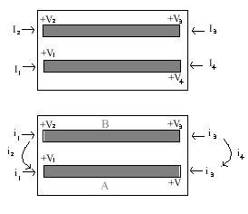
figure 8: a)a parallel coupled line b) even and odd mode currents
Filter characteristics of a single quarter wave coupled line: To find the open circuit impedance matrix we will consider even and odd mode excitations separately, then find the result by superposition. I1, I2, I3, I4 are the total port currents. i1, i3 are the currents driving the line in even mode, i3, i4 are in odd modes. Note that VA1 ,VB1 voltages on line A and B due to the current i1, VA2 ,VB2 voltages on line A and B due to the current i2, VA3 ,VB3 voltages on line A and B due to the current i3, VA4
,VB4 voltages on line A and B due to the current
i4. At the even mode, the impedance seen from ports 1 and 2 is Zein=-jZoe cot b l. (21) The voltage on the line can be expressed as VA1 (z)= VB1 (z) =Ve+[e-jb (z-l)+ ejb (z-l)]=2Ve+ cosb (l-z), (22)
The voltages at port 1 and 2 is for z=0; VA1
(0)= VB1 (0)=2Ve+cos b l=i1
Zine
Using (21) in (23), V(z)=-jZoe In the same way voltage equation can be written in terms of i3 VA3
(z)= VB3 (z)=-jZoe Zoin=-jZoe cot b l. (26) VA2
(0)=- VB2 (0)=2Vo+cos b l=i2
Zino Using (26) in (28), VA2
(z)=- VB2 (z)=-jZoo In the same way voltage equation can be written in terms of i4 VA4
(z)=- VB4 (z)=-jZoo Using the voltage equations the voltage at port 1 is found as (z=0) V1= VA1 (0)+VA2 (0) + VA3 (0)+VA4 (0) (30) Also total currents on the line can be expressed in terms of even and odd mode currents: I2=i1-i2, I3=i3-i4, I4=i3+i4. (31) i2=0.5(I1-I2 ), i3=0.5(I3+I4 ), i4=0.5(I3-I4 ), V1=-j0.5(Zoe(I1+I2 )+Zoo(I1-I2 ))cotq -j0.5(Zoe(I3+I4 )+Zoo(I4-I3 ))cscq (33) from symetry z-parameters can be found Z11=Z22=Z33=Z44=-j0.5(Zoe+Zoo)cotq , Z12=Z21=Z34=Z43=-j0.5(Zoe-Zoo)cotq , Z13=Z31=Z24=Z42=-j0.5(Zoe-Zoo)cscq , 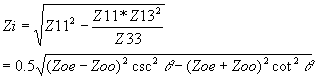
We can analyze the filter characteristic by calculating the image impedance (Zi) and the propagation constant.
When q goes to 0 or pi, Zi goes to infinity; meaning that stop band. Cut off frequency from (35) cosq1=-cosq2=(Zoe-Zoo)/(Zoe+Zoo) (36) Also propagation constant is determined by cosb =
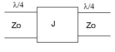
Design of Coupled Line Band pass filters: A coupled
line can be modelled by two transmission line and an admittance inverter
in between as shown in figure 8.
figure9:Equivalent circuit for coupled line
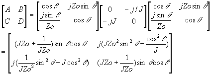
Firstly, let us compute ABCD matrix for this circuit:
Choosing
q =p /2, we can find The propagation constant is from the matrix
Using (35) and (39) Solving (41) and (42) we obtain even and odd impedances Zoe=Zo[1+JZo+(JZo)2 ], Zoo=Zo[1-JZo+(JZo)2 ], Now,
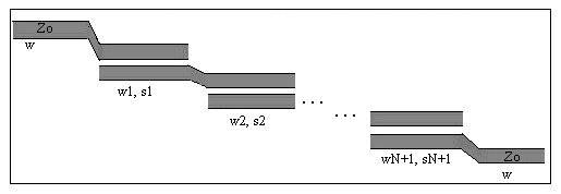
we cascade N+1 coupled line as in figure 9
figure 10:Cascaded coupled lines 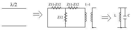
figure 11: Equivalent circuit for a transmission line with length l /2.
figure 12:Equivalent circuit for admittance inverter
If we equate it to the ABCD matrix of transmission line with length l/2 we can find the following Z12=jZo/sin2q Z11=-jZocot2q Z11-Z12=-jZocotq the transformer in the equivalent circuit (Fig 11) shifts the filter response without changing the amplitude so we can eliminate it. Then we have left with T network. For w=wo+Dw where wo is the center frequency 2q=bl=( wo+Dw )p/wo (45) for q~p/2 the series arms impedance of T network become zero, parallel arm impedance is Z12=jZo/(sinp(1+Dw/wo))~-jZowo/(p(w-wo)) (46) The impedance of parallel LC circuit near resonance is given by Z= Z= Using wo2=1/LC Using inductance and capacitance values following design equations can be derived
By using
(43), even and odd impedances of each coupled line can be found Finding geometry ratios by using even and odd impedances: Cascaded coupled lines can be realised in microstrip or stripline form.
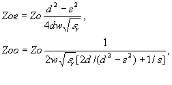
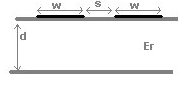
figure 13: Coupled stripline Stripline: For the geometry in figure 13, even and odd impedances are given by
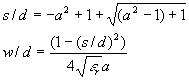
Using (48) we can derive s/d and w/d ratios:
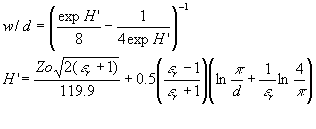
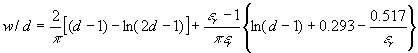
figure 14: Coupled microstrip Microstrip:
to find the ratios for microstrip is more laborious to carry out. Here
I used Akhazard method. Zose=Zoe/2 Zoso=Zoo/2 for single microstrip Using even and odd impedances for a single line we can find w/d ratio, For narrow
strips Zos {44-2er}
for wide strips Zos {44-2er}
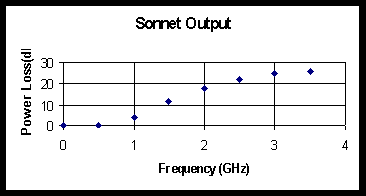
A DESIGN EXAMLE AND COMPARISON: I run the program for a low pass filter power loss of 15 dB at 2 GHz and cut off frequency at 1 GHz. The filter impedance is chosen as 50 ohm. The highest and the lowest practical impedance values are 150 and 10 ohm respectively. The output of the program for e=2.2: Lengths of lines w/d ratios l1 =0.64cm w1/d= 22.65 l2 =14cm w2/d=0.33 l3 =0.64cm w3/d=22.65
|
|||||||||||||||||||||||||||||||||||||||||||||||||||||||||||||||||||||||
|
Please contact our Webmaster with questions or comments. Webmaster: M. Irsadi Aksun |

 (9)
(9)
 (12)
(12)
 (13)
(13)
 (14)
(14)
 (15)
(15)
 (38)
(38)
 k=2,3�N (47)
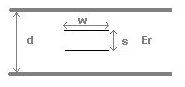
 (48)
(48)
 where a2=Zoe/Zoo
 where
d=59p2/(Zoer1/2)
where
d=59p2/(Zoer1/2)